Researchers at the National Institute of Standards and Technology (NIST) and at the University of Maryland have developed a step-by-step recipe to produce the atomic-scale devices. Using these instructions, the NIST-led team has become the second in the world to construct a single-atom transistor and the first to fabricate a series of single-electron transistors with atom-scale control over the devices’ geometry.
These type of transistors with only a few atoms have a lot of potential but to understand it completely scientists have to fabricate a lot of these devices which is difficult but this new research shows some hope.
The scientists showed that they could adjust the rate with which electrons flow through a physical gap or electrical barrier precisely in their transistor even though classical physics would forbid the electrons from doing so because they lack enough energy. That strictly quantum phenomenon, known as quantum tunneling, only becomes important when gaps are extremely tiny, such as in the miniature transistors.
The Fabrication Procedure
To fabricate single-atom and few-atom transistors, the team improved on a known technique in which a silicon chip is covered with a layer of hydrogen atoms, which readily bind to silicon. The fine tip of a scanning tunneling microscope then removed hydrogen atoms at selected sites.
The remaining hydrogen acted as a barrier so that when the team directed phosphine gas (PH3) at the silicon surface, individual PH3 molecules attached only to the locations where the hydrogen had been removed (see animation). The researchers then heated the silicon surface. The heat ejected hydrogen atoms from the PH3 and caused the phosphorus atom that was left behind to embed itself on the surface. With additional processing, bound phosphorous atoms created the foundation of a series of highly stable single- or few-atom devices that have the potential to serve as qubits.
The NIST team improved this method with two steps
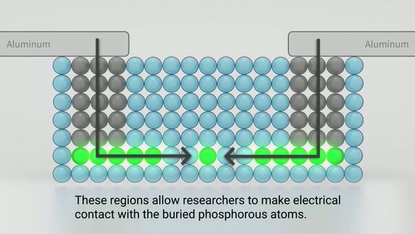
- Sealing the phosphorus atoms with protective layers of silicon
- Making electrical contact with the embedded atoms
These two additions appear to have been essential to reliably fabricate many copies of atomically precise devices, NIST researcher Richard Silver said.
“We believe our method of applying the layers provides more stable and precise atomic-scale devices,” said Silver. Having even a single atom out of place can lead to difference in the conductivity and other properties of electrical components.
The team also developed a novel technique for the important step of making electrical contact with the buried atoms so that they can operate as part of a circuit. The NIST scientists gently heated a layer of palladium metal applied to specific regions on the silicon surface that resided directly above selected components of the silicon-embedded device. The heated palladium reacted with the silicon to form an electrically conducting alloy called palladium silicide, which naturally penetrated through the silicon and made contact with the phosphorus atoms.
This process by which they made contact is being considered a major achievement of the research.
So, let us wait and see how these few atoms transistors change the scale of technology.
Journal
Atom‐by‐Atom Fabrication of Single and Few Dopant Quantum Devices : DOI: 10.1002/adfm.201903475